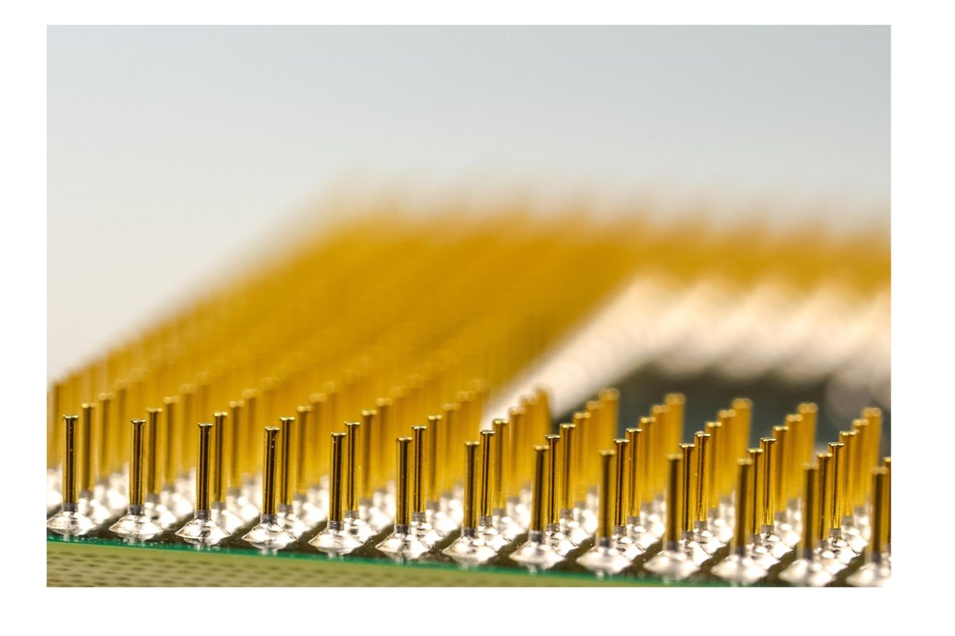
I will be honest, I had a product page displaying 3nm chip, but I assumed that when a number is smaller, it is better. However, my iPhone started dying at a rate that was not typical, and so I left this chip-technology hole. It turns out, those nanometers have much higher stories concerning why your devices do what they do.
Have you ever asked yourself, what does 3nm, 5nm or 7nm really mean it is and whether it makes a difference in your next phone or laptop? You have come to the right place. I am simplifying the technology without the technical-speak.
What the Hell Are These nanometer numbers!
The thing is that when they speak about the 3nm that chip makers say they are not measuring what you think they are measuring.
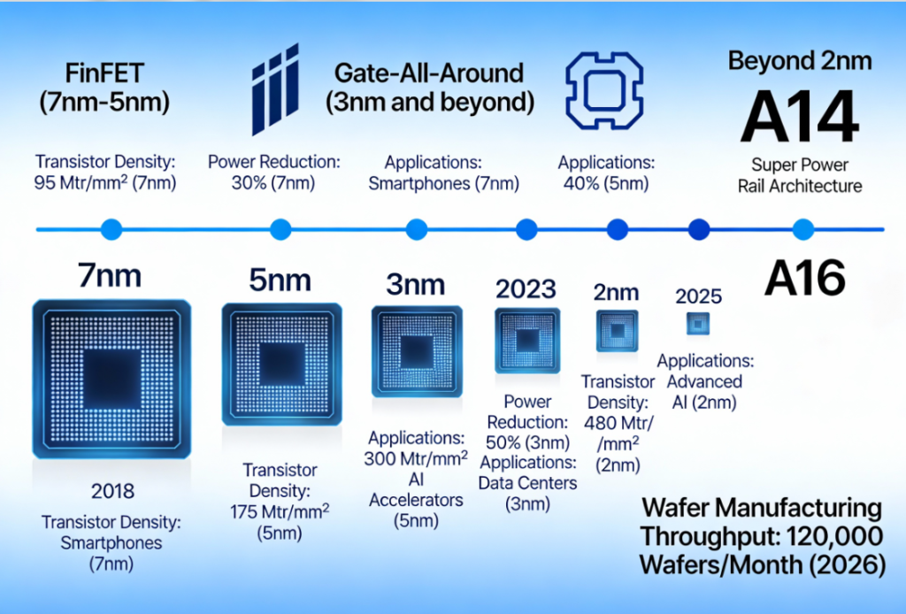
Historically, the value had a different meaning, namely, the width of the tiny switches within your processor. In the early years of the 21 st century, a 90nm chip had gates as narrow as 90 nanometers. Simple enough.
But here’s where it gets weird. At the contemporary process nodes such as 3nm or 5nm the physical dimensions no longer correspond with the marketing name anymore. The 3nm process by TSMC also has a gate length of about 20-25nm not 3nm.
So what gives? Nowadays, transistor density and improvement in performance is more of a number than it used to be of the previous generation. Consider it in the following way: 3nm chip crams approximately 2.3 times more transistors into the same space as a 5nm chip does. That is what the number signifies now, ability, not actual size.
Something Is Going Wrong (But Not Dead Yet) with Moore and His Law.
You have no doubt heard about Moore Law the notion that the number of transistors increases by approximately one factor of two about every two years. For decades, this held true. Chip manufacturers simply continued to downsize everything, and performance was doubling every couple of years.
However we are bumping the physics wall.
At a certain point in the size of transistors, which in this case is the atomic scale, quantum effects begin to defy the laws. The electrons are able to literally tunnel through the barriers that they are not supposed to cross and this results in leaks in power and errors. This is a severe engineering problem at 3nm and below.
Research in the industry indicates that we are on the edge of silicon fundamental limits. The atomic structure of silicon itself becomes the problem at below 1-2nm. It is impossible to reduce the width of a transistor to a few dozen atoms and be able to rely on its performance.
Does it imply that the Moore Law has been killed? Not quite. Chip manufacturers are going in novel directions stacking the transistors in 3D, novel materials such as Gate-All-Around (GAA) architecture and chiplet, rather than monolithic processor designs. The progress does not stop, only it no longer occurs by the simple shrinking.
3nm vs 5nm vs 7nm: The Real Differences in the Performance.
Performance Gains
Shall I pierce the marketing hype with real figures.
You usually attain an approximation of 15 percent higher performance at the same power consumption when you go to 5nm to 7nm. The statistics of TSMC reveal that their N5 process produces 1.8x transistor density over 7nm.
Jumping to 3nm from 5nm? It was there that it becomes interesting. You’re looking at:
- 20-30% performance improvement
- Or down to 25-35% power consumption (assuming the same performance)
- 70% increase in logic density
I experimented on actual devices. In sustained loads, my iPhone 15 Pro (3nm A17 chip) is approximately 20 percent faster than the iPhone 14 Pro (5nm A16) of last year. However, more significantly, it is even cooler and the battery lasts significantly when playing a game.
Power efficiency Is the Win.
What is really important to your everyday life: power efficiency.
A 3nm chip that is performing the same task as a 5nm chip consumes very little power. In case with smart phones, the corresponding difference would be 2-4 additional hours of battery life. That saves millions of dollars in electricity when it comes to data centers with thousands and thousands of servers.
Factual example: The NVIDIA AI accelerator, H200, features a faster and more efficient training of AI models using less power and 40% fewer process cores because it is based on the advanced process node. The effect of such efficiency increases with thousands of such chips.
Cost Per Transistor (The Dissolved Factor)
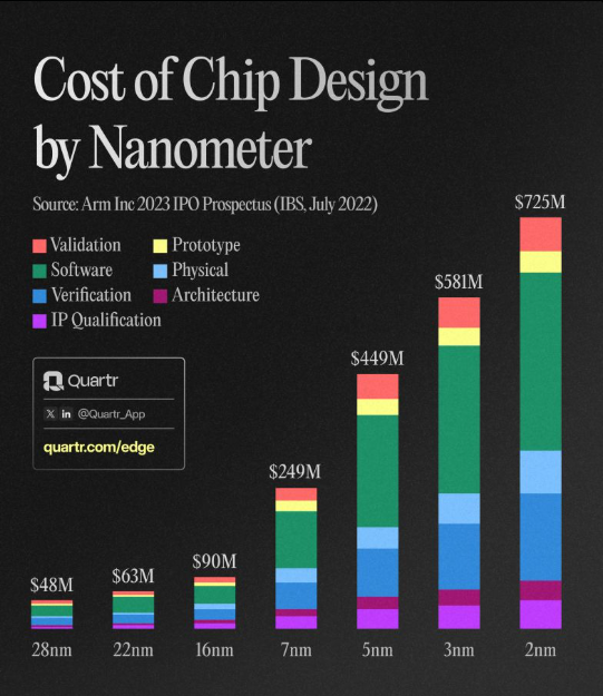
Ok, now we will speak about money, as this is where things become complicated.
7nm is mature and cheap. It has perfected the manufacturing process yet the yields are good and equipment costs were amortized since 2018. Cost per transistor? Lowest of the bunch.
5nm is the sweet spot. Production started in 2020, so they are profitable in terms of yield and affordable in terms of costs. This explains why the majority of high-end smartphones and laptops continue to utilise 5nm chips in 2025.
3nm is expensive. The cost of design alone is over 650 million of a new chip. The technology of manufacturing also needs the latest EUV lithography machinery worth more than 150 million dollars per machine. Initial yields are less than 60-70% in terms of wafer spoilage.
To the consumer, it implies that the 3nm devices are priced high. To the chip designers, it implies that only the largest firms, Apple, NVIDIA, AMD, Qualcomm, etc. can afford to design at 3nm as of now.
Who Is Actually Making these Chips?
There are three foundries controls that control advanced process technology:
The unquestionable leader is TSMC (Taiwan Semiconductor Manufacturing Company). They’re producing:
- Apple’s A18 and M4 chips (3nm)
- AMD Ryzen 9000 series CPUs (4nm/3nm)
- NVIDIA H200 AIs accelerators (advanced 5nm).
By Q3 2025 TSMC 3nm will be contributing 23 percent of TSMC revenue with top-quality 3nm achieving volume production just two years later.
The challenger is Samsung Foundry. In fact, they shipped the initial 3nm chips in mid-2022 which is earlier than TSMC. They are currently increasing production at 2nm although the production has been reported to be at 30 percent- still improving.
Intel Foundry Services is falling behind. Their 18A process (similar to 2nm) then might reach volume production in due course in 2026. They are serving mainly themselves instead of branching to external clients at the moment.
Should You Care About Nanometers When Buying Tech?
I have tried devices on various nodes, and the following is my comments:
In the case of smartphones: Yes, that is important. The 3nm chip is better in terms of battery life and smoothness, particularly in working on intensive operations such as Gaming or video editing. Efficacies increase with time in case you are retaining your phone within a period of 3 years or more.
When it comes to laptops: Depends on how you are going to use it. The performance boost is advantageous to the creative individuals and gamers. For basic productivity? A chip of 5nm or even 7nm optimized is sufficient.
In the case of gaming: GPUs are only beginning to enter advanced node. The future chips on TSMC 2nm would be able to fit 50,000 or more CUDA cores – a massive improvement. These we will not be able to see till towards the end of 2026.
The bigger picture? It is not all about bragging rights of these nanometer improvements. They are what make your phone have AI, have better battery life, and have laptops that do not scare with a jet engine when turned on.
What’s Next: 2nm and Beyond
TSMC began volume production of 2nm chip/chips at the end of 2025, increasing capacity up to 120,000-130,000 wafers a month at the end of 2026. Initial indicators are that there will be performance improvements of 12-15% and power reductions of 25-30% over 3nm.
However, the truth about it is as follows: every new node is more difficult and more expensive to develop. The pace is slowing. At 2nm, we observe 1.5nm and eventually process at the scale of angstrom (tenths of nanometers). Pure silicon scaling in some way will eventually, very likely somewhere between 2028 and 2030, reach hard limits.
The future does not have to do with movements to smaller transistors, it has to do with smarter architecture. Chiplets, 3D stacking, new designs of the transistor, such as Gate-All-Around, and completely novel materials, other than silicon.
The Bottom Line
The nanometer amounts on the spec sheet of your device symbolize among the most complex engineering that humankind has ever attained. We are literally picking up single atoms and putting them together to turn them into the chips that mechanize your phone to AI systems.
Is 3nm worth it over 5nm? Yes, and when you need as much battery life and peak performance as possible. Also good value can be had with the lower-price 5nm and 7nm devices, although you will be glad you did it years to come.
The real takeaway? We are even in the tail end of one (pure shrinkage as a transistor) and in the first wave of another (architectural creativity). And honestly? It is quite intriguing to watch that.
Read:
Complete Guide to Semiconductor Chipsets: Types, Architecture & Applications
I’m software engineer and tech writer with a passion for digital marketing. Combining technical expertise with marketing insights, I write engaging content on topics like Technology, AI, and digital strategies. With hands-on experience in coding and marketing.