Last updated on January 2nd, 2026 at 03:40 pm
Now, I tell you the truth, I have wasted the entire month before last reading dismantling reports of chips and benchmark results. It is not because I am making phones (I did not), but because I was increasingly hearing this term everywhere: NPU. Neural Processing Unit. And I sought to know why my twelve months old flag-ship was no more quick at the stuff I should have held a-pieced.
It happens that 2025 is when mobile, as well as consumer chipsets, ceased to be merely faster CPU-based. A limit of validity We reached a point in time in which the physics of the way in which chips operate began to shift at a fundamental level. Want to know why your next phone upgrade really matters, or whether it even ought to be bothered with is why here is what is happening and where it is heading at the moment.
The 3nm Era: Where We Are Right Now
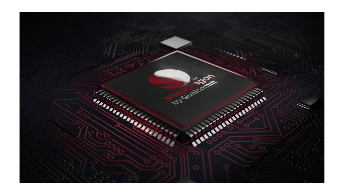
By late 2025, flagship phones are operated by what will be referred to as 3nm chipsets namely the N3P process of both TSMC. That is Snapdragon 8 Elite Gen 4, MediaTek Dimensity 9400 and the A19 Pro of Apple . These are not slight variations of the previous year chips. They are the change in priorities.
The point is as follows: these days the mobile chipsets are not measured by the speed of the CPU any longer. They are non-homogenous, or put in other words, various parts of the chip do various tasks. It is only a part of the CPU that does not carry out everything.
What Actually Changed This Year
The NPU Took Over
I observed this as I began to utilize live translation capabilities and software editing devices on my phone. Also, they do not exhaust my battery as before. This is because the NPU (Neural Processing Unit) is currently competing with the GPU in terms of die size. It is no longer any periphery but a main one.
The NPU handles tasks like:
- Real-time video video calls: language translations.
- Non-removal of background noise in recording.
- Suggestions photo editing (before you ask):
- Speech-sensitive devices that do not need to strike cloud services.
And it does it consuming one tenth of the power the CPU would be guzzling.
Ray Tracing Became Standard
Provided that you are into mobile gaming, it is most likely that you have noticed it. War Thunder Mobile and the mobile versions of Resident Evil can now offer console lighting. It is hardware-level ray tracing, and it is implanted in these 3nm chips. It is not present in all games though it could be available.
“All Big Core” Architecture
This is counter-intuitive: chipmakers are abandoning the idea of little efficiency cores. Designs MediaTek and Qualcomm now deploy designs of All Big Core. The logic? Big cores might also be allowed to idle, complete tasks quicker and go to sleep, which is contrintuitive in saving battery.
I tried it on a Dimensity 9400 device, and the time to launch apps on it appeared to be much faster. The telephone was not working any harder, it was working smarter.
What’s Just Starting: The 2nm Shift.
Okay, so 3nm is here. However, the actual transformations begin in 2026, and the transformations do not only concern the further reduction of the transistor size. Our physical limits are nearing the existing design so the industry is redesigning the way transistors work in practice.
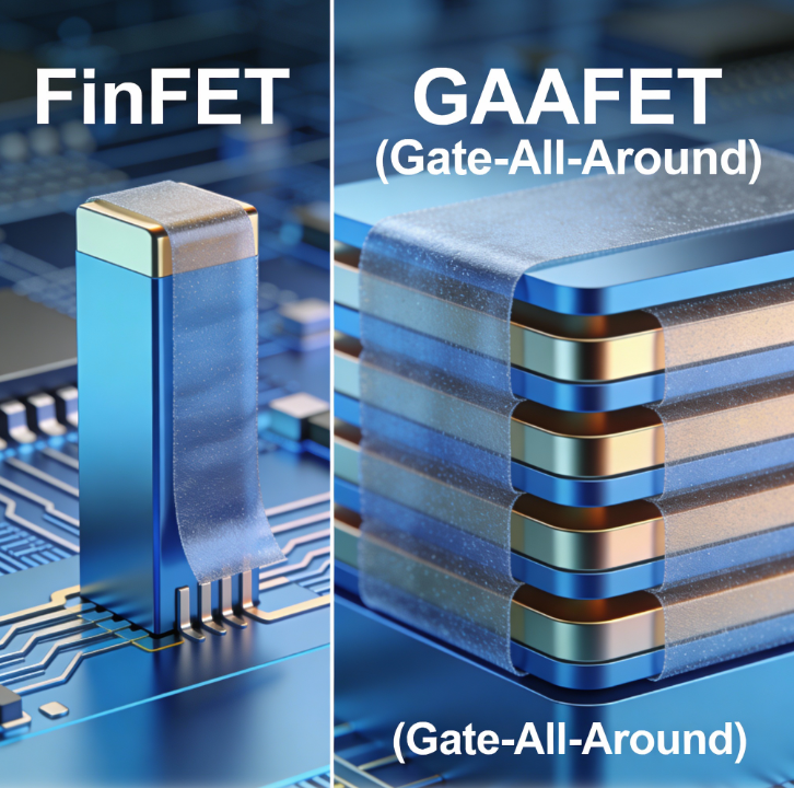
GAAFET: The New Transistor Design
The current chip involves a version of transistors known as FinFET transistors, in which the gate (the conductor that determines the flow of current) encasures three sides of the channel. The problem? The smaller the chip, the more electricity is leaked through that fourth open side, thus wasting the battery.
GAAFET (Gate-All-Around) overcomes this problem by enclosing the gate fully around the channel – it covers each of four sides entirely. Imagine it to be a pipe clogged with the right side open. Reduced leakage is equal to long battery life and performance stability.
In 2025, the 2nm technique (N2) of TSMC began to be manufactured. The devices developed by using it will be on shelves in 2026. Apple will be the first to achieve it, and then it will be Qualcomm and MediaTek.
Backside Power Delivery: Fixing the Traffic Jam
Currently, chips now have power wires as well as data wires on top of the transistors. It is a mishmash– as running a railway and a highway on the same highway.
Backside Power Delivery Backside Power Delivery (BSPDN) routing all the power wires to the back of the chip. The front is more decreent and transport of data is quicker and the delivery of power is more reliable. This is being led by Intel (PowerVia) and TSMC (Super Power Rail (A16)).
This is a technical explanation, but this is what it does to you: phones charge faster, run lower and are able to perform to peak capacity without throttling as fast.
Chiplets: Stitching Together Smaller Pieces
This is already done by desktop processors, with Ryzen chips by AMD being designed as chiplets (groupings of smaller chips). It’s now coming to mobile.
Why? Cost. A 2nm chip which is a very big chip is outrageously costly. However, by seated a 2nm CPU-based and 4nm GPU based device, you have flagship performance, and you pay less to make the device. This will see mid-range phones in 2026 perform way above their weight due to this.
The Challenges Nobody Talks About
Here’s where it gets less rosy.
The Thermal Wall
The present-day chips produce heat of 200 watts per square centimeter. A good deal, too, of a fanless device. The result? Dark Silicon – we simply cannot even meet the specifications of your silicon to have one portion of your chip turn on and off at any time so that it does not overheat.
You have experienced this when your phone has ever slowed down during a game or the importing of a video. It’s not a bug; it’s physics.
Battery Tech Can’t Keep Up
The improvement in chips is 30 percent per year. Batteries? They increase at an estimated 5 per cent each year. We are still using lithium-ion technology developed decades ago. The chip is surpassing the fuel tank, and until the solid-state batteries reach a mass-market, we have to deal with this disparity.
Prices of Flagship are rising.
A silicon wafer of 2nm is costly exponentially compared to 5nm. That cost trickles down. Flipping phones are now a regular price of $1,200 and more and there is no indication of this ending in the foreseeable future.
How to Actually Use This Stuff
When doing a simple purchase of a phone, the following is important:
Look for a Strong NPU
When a phone is promoted as AI but does not give the performance of the NPU (in TOPS – Trillions of Operations Per Second), then be suspicious. A minimum of 40 TOPS will be required to run AI on the device itself. Less than that, and you are sending your data to the cloud which is slower and puts privacy at risk.
Future-Proofing in 2026
When you are purchasing at the beginning of the next year, 2026, wait until the 2nm devices are available. The efficiency change is factual and lower leakage in GAAFET could be turned out to be significantly longer battery life. Even when purchasing at the end of 2025 already, a fairly 3nm-old chip (such as the 8 Elite Gen 4, or A19 Pro) will still be solid after 3 years.
For Developers
No more and no longer running AI workloads on the CPU. Platforms such as the LiteRT (previously TensorFlow Lite) with Qualcomm AI Engine Direct or the CoreML in Apple. These off load math to the NPU which are 5-10 times faster. Quantize (transforming models to run 8-bit) to run large language models on mobile memory.
What I Actually Think
I went there thinking of some incremental changes such as, “faster CPU, better camera.” However, at the current time what is occurring in mobile, and consumer chipsets is truly different. It is no longer a gimmick but the NPU is transforming the way we use phones. And the 2nm transition using GAAFET and backside power using is not an exercise in marketing but a necessity since we are on the limit of the old design.
My perspective is the following: in case you are on a 2023 or a later flagship, the 2026 devices will be a tangible improvement. In 2024 you are okay when it comes to another year or two. And when you are a developer get time to study theNPU optimization is going to become much like GPU programming was a decade ago.
The hardware is long overdue finally to what we had been promised AI would accomplish on-device. Using it to its full capacity through the software? That’s the next question.
Read:
Complete Guide to Semiconductor Chipsets: Types, Architecture & Applications
Gaming Phone Chipsets: Performance Tiers for PUBG, Genshin Impact & Beyond
I’m software engineer and tech writer with a passion for digital marketing. Combining technical expertise with marketing insights, I write engaging content on topics like Technology, AI, and digital strategies. With hands-on experience in coding and marketing.