Last updated on December 27th, 2025 at 08:14 am
I didn’t know, I would have said they were all the same. A chip is a chip, right? Then I began to delve into why the new CPUs of AMD are slaughtering Intel in some benchmarks, and why AI chips of NVIDIA are as expensive as second-hand vehicles.
It happens that the semiconductor industry as a whole is experiencing the largest architectural transformation in decades and changing not only your gaming computer but also the servers to ChatGPT are being impacted.
This is what is actually happening to chipset architecture, why it is significant, and the implication on the very technology you are currently purchasing.
The Old Way: Monolithic Chips Explained
All of computer history before most of its history, the processors were monolithic; that is, a single piece of silicon with everything built into it. Your processor units, graphics, cache RAM, I/O controllers, all of it made on the same unit and made with the same process.
Stampede The idea is, construct a house with a single large concrete pour. It is all interconnected, ultra-tight all the rooms and there has been no lag between rooms since it is all the same structure.
The upside? Performance is incredible. When a complete signal chain is on a single die, communication takes place in x30 seconds and it produces very low latency. Power control is also easier, you are only managing a single piece of silicon, not managing a number of parts.
The downside? Cost and size are monstrous issues, as the sizes of chips increase.
This is interesting as it is here that the chip manufacturing uses what is known as reticle limit, or, in other words, the biggest size that you can print the silicon in a single shooting. The closer you come to that limiting design the more yah collapse in the economics. A single flint of that gigantic die? The entire chip is trash.
I have counted the updating of this, and it is crazy. Assuming a 800mm2 monolithic processor, and assuming you have a defect rate of 0.1/unit area in your manufacturing process, your yield (percentage working chips) will have fallen below 50. Fifty percent of what you make goes to the trash.
What Makes a System-on-Chip (SoC) Tick
Talking about what is really inside these things, we shall get to the chiplets before we do anything about them. The SoCs of the modern world consist of insane functionality in a single package.
CPU cores can perform the general compute: The web browsing, application logic, daemons. They are the most developed part, and they are made based on the latest nodes of processes such as 3nm or 5nm.
Graphics and parallel calculation is handled by cores of the GPU. Phones currently have specific hardware in the form of a GPU since on-demand Instagram filters have intensive horsepower requirements.
Memory hierarchy comprises of several levels of cache (L1, L2, L3) which are super-fast storage that are practically onboard in the same place as your processing cores. One such example as 3D V-Cache by AMD actually build additional cache on top of the CPU literally.
I/O controllers deal with all the ingress and egress such as USB connection, PCIe lanes, network, and display. These do not require the state of art transistors, processors of a more ancient cheaper type are fine.
Special purpose architecture The Digital Signal Processor (DSP) used in audio processing, Neural processing unit used in AI processing, and camera image signal processing. The A17 Pro produced by Apple has an exclusive 16-core Neural Engine to specifically handle machine learning.
This separation of responsibilities amongst the CPU, GPU, and NPU underscores why each processor is made to perform a certain task a difference that has been discussed in detail in the article CPU vs GPU vs NPU: What is the Difference and When to Use Each.
The challenge? You are putting all that on a single die manufactured in a single manufacturing process and that implies you are putting in the costly 3nm transistors on what could perfectly on a cheaper 12nm or 16nm manufacturing process.
The Chiplet Revolution: Razing Things.
A chiplet architecture is used instead of a single giant die and divides your processor into smaller and modular units that are then packaged together to form one chip.
I was doing a research about Ryzen 7 9700X3D and stumbled upon the technique of AMD and it made sense. They are incorporating individual chiplets of CPU cores and I/O, and linked by an internal fabric. Their newest 5nm process is used on the CPU chiplet, and older, cheaper, 6nm or 12nm node is used on the I/O die.
This mix-and-match strategy is directly related to the idea that the selection of different process technologies such as 3nm, 5nm and 7nm is based on performance requirements rather than cost of manufacture, a trade-off that was explored in detail in the article titled, Understanding Chip Process Technology: 3nm vs 5nm vs 7nm Explained.
Why this changes everything:
The yield economies are radically improved. Four 200mm2 chiplets with 85% yield are used instead of a single 800mm2 die with 45% yield. In the case of one of the emergent defects, you can always discard a tiny part not the whole processor.
Process nodes can be combined and interchanged. Put bleeding-edge 3nm where CPU cores are important, mature 12nm where I/O controllers are not. As a result of this flexibility, the price per transistor of advanced nodes is 3-5x higher.
Customization is made possible by modularity. Want more cache? Alternate cache chiplet. Need better AI performance? Install a neural processing chiplet. It is the construction with LEGO rather than the connection with marble.
Real-Life Examples Monolithic vs. Chiplet.
The highest level of monolithic design is Apple A17 Pro. All CPU, GPS, Neural Engine, memory controllers, image processor are all crammed on a single 3nm die. It is reasonable in the case of a phone chip where space is of absolutely paramount importance, and the overall die size is reasonable. It is unbelievable how much power it can save, and Apple is able to optimize all the connections it has in order to achieve maximum performance.
But go large-size to a server processor or high-end desktop chip and the economics fail.
AMD Ryzen 7 9700X3D chooses the path of chiplets. Processing is done in the compute dies, and memory and external connections are processed in a different I/O die. AMD goes as far as to add more cache to the chip via 3D packaging technology. It will be too costly and too low-yielding as a monolithic chip, but as chiplets, it becomes economical.
The variance reflects itself in pricing and performance scale. AMD is able to sell 16-core processors, 32-core processors, or even 64-core processors by just adding increased chiplets. Attempt to create a 64 core monolithic die and you will be looking at single digit yields- provided that it can be made at all within manufacturing constraints.
The Tech That Makes Chiplets a Possibility.
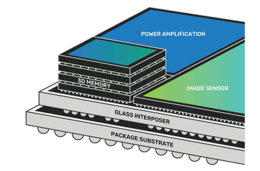
You can not simply hit chiplets and be done with it. They require very high speeds which is where superior packaging comes in.
CoWoS (Chip-on-Wafer-on-Substrate) offered by TSMC is the gold standard of the AI chips such as the NVIDIA H100. It deposits chiplets on a silicon interposer- fundamentally a passive slab of silicon with microscopic circuits through which large amounts of bandwidth can be passed amongst dies. Imagine it is a circle of silicon and not fiberglass circuit board that is overloaded.
The EMIB (Embedded Multi-die Interconnect Bridge) by Intel is more affordable. In place of a massive interposer, Intel incorporates miniature silicon bridges where chiplets literally must communicate. It is less expensive and more consumer product wise.
The stacking is made vertical in the 3D. V-Cache is the actual connection of the literal attachment of additional memory over the CPU die by AMD, making the hopscotch of signals almost negligible. The performance increases documented by the 3D V-Cache were legitimately staggering when I first encountered the gaming performance benchmarks, and in some games, were as great as 15-30% simply because there was a cache nearer to the cores.
The Interconnect Standard: UCIe.
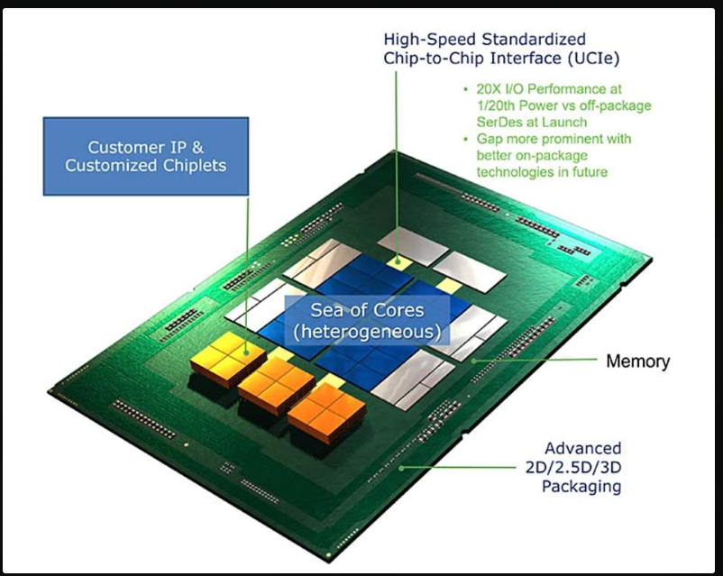
This is where it is really interesting to the future. UCIe (Universal Chiplet Interconnect Express) is an open standard supported by Intel, AMD, NVIDIA, TSMC, and, effectively, all the players in the semiconductor industry that count.
It’s like USB for chiplets. Rather than each company having setups that connect them to that particular standard, UCIe identifies a standard interface that allows chiplets across manufacturers, in theory, to communicate.
The implications? A start-up may create an AI accelerator chiplet, and a system integrator may edit it with an Intel CPU and an AMD graphics card. We are not that far–yet this is early days–but the groundwork is being made this very moment.
Manufacturing Reality: Why This Matters
It is not merely a matter of design or performance the change to chiplet. It essentially comes to a dead of economics and physics.
The smaller the transistor, the below 5nm, the harder and more costly it is to manufacture. One EUV lithography costs above 150 million. Defect rates increase. Yields drop. The only solution is to scale big, and complex processors down to small sized processes that yields can be managed.
Besides it does not have to be cutting-edge transistors. I/O controllers are capable of working with 12nm processes in 2017. It simply could not make economic sense to pay 3nm transistors on your whole chip merely because 70 percent of it will not be useful to you.
I have had a conversation with a friend who was a hardware engineer doing work in the space, and the conversation with him was bluntly straightforward: Monolithic is dead above a phone chip. The industry isn’t going back.”
What This Means for You
Even when you are purchasing a CPU at the present moment, you are already making the decision between these architectures at least unconsciously.
In the case of laptops and phones: Monolithic is victorious. The intra-company strategy by Apple offers superior battery life and optimization of small devices.
Desktops and servers: Chiplets prevail. The Ryzen and the EPYC chips are AMD, the future processors designed by Intel, they are all headed this way since it is the only way to scale performance and the cores cost-effectively.
In the case of AI and data centers: Chiplets are a necessity. The NVIDIA H100 would not be possible without the advanced packaging of giant GPU chiplets to a fast memory.
The following five years will be regarding optimization of the interconnects, better thermal handling (heat in 3D stacked designs is a nightmare) and interfaces standards such that chiplet of one vendor can actually communicate with chiplets of another vendor.
The Bottom Line
The current trend in chipset architecture is the transition to chiplet design since the previous method of design could not deliver any more. The change is imposed by physics and economics, and the whole industry is changing.
Monolithic chips will still persist in mobile device and app use where integration and power efficiency are far more important than other factors. However, in the case of high-performance computing, such as, gaming, AI, servers, or workstations, the future lies with the chiplets.
It is the frankly one of the biggest shifts in computing structure in decades, and it is currently being done. These CPUs and GPUs of 2026 and beyond will be constructed in a format like this, and it is important to understand the transition so that when your next processors change performance features dramatically you will understand the rationale.
Interesting to listen to, particularly when you are buying any hardware or assembling something that includes some state-of-the-art silicon.
Read:
Complete Guide to Semiconductor Chipsets: Types, Architecture & Applications
I’m software engineer and tech writer with a passion for digital marketing. Combining technical expertise with marketing insights, I write engaging content on topics like Technology, AI, and digital strategies. With hands-on experience in coding and marketing.