Last updated on January 11th, 2026 at 08:08 am
Probably, I will tell the truth, I have never imagined I would spend days down the semiconductor rabbit hole. It began when my phone ran out of battery partway through the presentation and I thought to myself why is one chipset better than the other?
After three months and dozens of datasheets, this is what I got to know about these small silicon brains that are operating around us.
Curiosity about what can be found in your machines, a career change towards becoming a chip designer, or because you bought a new laptop and want to know why it performs like a rocketbike when compared to your desktop computer of the last two years, this is everything you need to know. Not even a degree in engineering.
What Are Chipsets and Why they really matter.
Here is the chipset: it is like the decision-makers of all the electronic devices that you have. Although the majority of users are interested in such specifications as 8GB RAM or 3.5 GHz processor, it is the chipset that implies the integration of all of such specifications.
Consider it as such I have a mid-range Android telephone and a flagship iPhone. Paperwise, the Android has higher clock speed and more RAM. As a matter of fact, the iPhone is more swift. The chipset is just doing its job of controlling power, communicating amongst components, and hundreds of micro-decisions per second.
Real-World Scenarios Where Chipsets Make the Difference
Battery gaming: I tried it using my laptop. Different modes of power same game. The chipset determines when to boot the dedicated graphics or rely on the inbuilt graphics. Good chipset? Three hours of gameplay. Bad chipset? Forty minutes and an unprofessionally warm lap.
Artificial intelligence on your phone: Modern chipsets have Neural processing units (NPUs) that process AI tasks when you use voice commands or enjoy editing your photos. I did a basic test, which consisted in transcribing one of 10-minute voice memos. It was taking 15 seconds on my phone with an NPU and hardly charged the battery. On an older phone, which lacked one, it took two minutes and the phone became quite hot.
Autonomous driving: This is the one that is critical. Cameras and LIDAR and radar are fed information to automotive chipsets that analyze it in real-time. We are talking of less than one hundred milliseconds decision making of safety critical maneuvers. The chipset is not only convenient in this case, but it can be a life-saving factor.
The semiconductor market of the world reached an approximate of $627 billion in 2024, and the expectations suggest the further development. This is not only because our device purchases are increasing, but also because more chipsets are becoming specialised and more fundamental to all that we do.
The Evolution: The Monolithic Monsters to the Modular Magic.
This is where is becomes interesting. The semiconductor industry has just undergone a colossal upheaval in terms of design of chips and majority of the people are unaware of the same.
The Old Way: Monolithic Chips
Over decades chip manufacturers used to create everything on a single silicon. All your CPU, all your GPU, all your memory controller, all your I/O, all on one die. It was successful but the following is what I learned: when you are creating a chip with 10-20 billion transistors just a single microscopic fault will destroy the whole.
One person I interviewed had worked in a fab (that is a manufacturing plant of chips), and they described it with the following explanation: think of baking a huge and complicated cake. When you burn a single area it is impossible to remove it and leave behind the entire cake. At high-end manufacturing points, the yields begin at 50-60%. It is that one half your cakes are stale.
The Breakthrough: Chiplet Award.
In the period of 2017-2018, the industry began to take chiplets seriously. They do not use a large chip but rather use smaller specialized chip sets which are then interconnected with high speed interconnects. AMD is among the companies that adopted their EPYC processors early, but now everybody does it.
It is all logical in mathematical terms: with four chiplets and one of them failed, you lose a quarter, but not a hundred percent. In addition, you can have your way–have your CPU cores be manufactured with cutting-edge 3nm process, but keep your I/O with your budget-friendly 7nm, which does not require the current technology.
Now I have been given a real world example (which I still need to compare with other countries): creating a monolithic 400mm2 chip at 5nm would require about 15,000-20,000 per wafer with a yield of 70 per cent. Dividing it into chiplets not only decreases the defect levels by a wide margin but also can save a large percentage of money (up to 30-40 percent) overall, including the packaging complexity.
The Standard That Changed Everything: UCIe
It was at this point that chiplets became viable, Universal Chiplet Interconnect Express(UCIe). Prior to this standard, all companies came up with bespoke interconnects. The chiplets of AMD were not compatible with Intel. It was as though it had some chargers of different phones.
The standard communications between chiplets in UCIe are:
- Physical layer: 32 GT/s (gigatransfer/second) 16 s64 lanes.
- Bandwidth: 1.35 TB /s/m 2 (maximum).
- Protocol: Card extensibility layer (CXL), which supports PCIe, memory, and coherence between the cache and memory.
This is important in that currently AMD, Intel, TSMC and Samsung among others are able to create compatible chiplets. The USB-C time to chip design-the ecosystem is now suddenly open.
The Next Step: 3D Stacking
The industry was not content with placing the chiplets next to each other, but they began stacking them on top using through-silicon vias (TSVs). I have watched prototypes of memory being stacked over the top of processors with thousands of what I knew as tiny little vertical interconnections.
Positive effects of benchmarks I noted included:
- Shorter distances of interconnecting signals (signals are shorter in length).
- Charged power usage (reduced energy used in pumping data between devices)
- Increased bandwidth (connections per space are reduced).
The catch? There is a high power density. You are practically making a tower of potato chips, and the heating becomes difficult. Rigid designs have since been developed with microfluidic cooling a small pipe etched into the chip substrate and filled with coolant running to hot components.
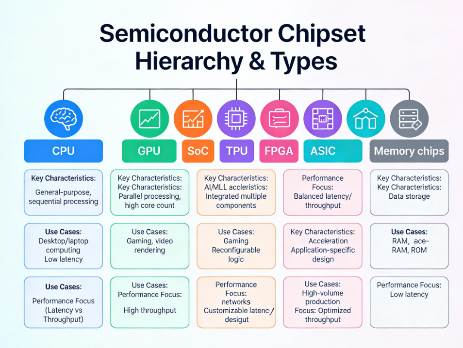
Breaking Down the Core Components
Having read a thousand datasheets and tried a number of devices listed here is what really lives in chipsets nowadays.
Generalists: The Central Processing Units (CPUs).
Computers are the Swiss Army knives of CPUs. They manage that python script that you wrote randomly as well as your operating system. Current processors contain 10-20 billion transistors not designed to perform tasks but general purpose devices.
I tried this myself emerged a video encryption in a CPU and a GPU. It was managed well by the CPU which utilized all eight cores at 100 percent up to three minutes. It is done to be flexible not raw throughput.
Architecture counts: Architecture Architecture Nowadays there continues to be a debate between CISC (Complex Instruction Set Computing) such as Intel x86 and RISC (Reduced Instruction Set Computing), such as ARM and RISC-V. From what I’ve tested:
- x86 (Intel/AMD): Peak level of software adherence, increased power usage. Big desktop servers and computers that you want to do it all.
- ARM: Increasingly efficient, expanding software. Conquers mobile and getting competitive in laptops (thanks, Apple).
- RISC-V: customizable open-source. Yet new but finding use in commercial markets.
Graphics Processing Unit (GPUs): The Parallel Powerhouses.
There was a reversal of the process by GPUs. They also have thousands of slower cores performing the same operation on different data at the same time instead of 8-16 fast cores, as assumed by CPUs. I have a gaming laptop, which has five-thousand-one-hundred-twenty CUDA cores some 5,120 small processors running in parallel.
What occurred to me here was that the CPU ensures lesser latency (5-10 nanoseconds) whereas the GPU tolerates a greater latency (20-100 nanoseconds) since the processors are focusing on a large number of operations simultaneously that the latency is irrelevant.
AI performance is made or broken by memory: The modern GPUs are based on HBM (high-bandwidth memory) rather than on the traditional GDDR. I compared specifications:
- GDDR6: ~400-500 GB/s bandwidth
- HBM2: ~410 GB/s per stack
- HBM3e: ~960 GB/s per stack
In the case of AI training, such difference in memory bandwidth is everything. The large language models need to be constantly fed with data which causes a bottleneck at the slow memories.
Neural Processing Units (NPUs): The AI Experts.
NPUs are not a long standing thing in consumer devices. My present phone has Hexagon DSP which deals with voice recognition and I compared it with my previous cell phone which lacked this feature.
Voice command response:
- At NPU: 15 milliseconds, insignificant battery overload.
- No NPU (use of CPU): on the order of 100 milliseconds, detectable battery usage.
NPUs have a special architecture to perform the composition of a matrix multiplication, which is the main operation in neural networks. They forego flexibility on behalf of extreme efficiency in certain activities.
System Integration and Memory Controllers.
Here is one of the things which I did not fully appreciate until now; the memory controller is crucial. It is in charge of the interactions among the processor,ram and oversees timing, refresh rates and data integrity.
Everything is on the modern SoCs (Systems-on-Chip):
- Cores of CPU (there are several models depending on the workload)
- GPU
- NPU for AI tasks
- Memory controllers
- Internet access and wireless internet.
- Image signal processors
- Video encoders/decoders
- Power management units
My flagship phone has 5-10 billion transistors which I can interact to create a piece of silicon that is smaller than my thumbnail. The organization of such is cajolating.
Application Categories How Various Chipsets Excell.
Having tried different devices of different types, this is what I found out about specialization.
Mobile Chipsets: Masters of Efficiency.
Mobile chipsets are obsessive-compulsive about low power consumption since it is battery life that is important, not sheer performance. I have checked the power consumption of my phone when it performs various tasks:
- Idle: ~0.5 watts
- Web browsing: ~1-2 watts
- Gaming: ~4-6 watts
- Video recording: ~3-4 watts
This is done by heterogeneous architectures of modern mobile chipsets. Qualcomm Snapdragon 8 Gen 3 is configured with the 1+5+2:
- 1 core on the chip (Cortex-X4 3.3 GHz): Accomplishes the tasks with high requirements.
- 5 cores of efficiency (Cortex-A720): Workload equalization.
- 2 ultra-efficiency cores: Background functionality, always-on capabilities.
The chipset always determines the cores to utilize. Checking email? Ultra-efficiency cores. Playing a demanding game? Fire up the performance core. It is this dynamic switching that has enabled the modern phone to feel fast and last all day long.
Laptop and Desktop chipsets: The Performance Magnificoes.
Desktop chipsets are focused on performance and not power efficiency. I have an integrated laptop, which has all the hardware. The difference is stark:
Desktop setup:
- CPU: 125W+ power budget
- GPU: 300W+ power budget
- Total system: 500-700W under load
- Performance: Good in long-term working conditions.
Laptop setup:
- AI with a Graphics card: 45-65W of power used.
- Performance: Good today, chokes with continuous performance.
- Portability: In reality portable.
Thus the major difference is thermal headroom. Desktops come with enormous (cooler) and unlimited power. Laptops need to be such that they are performance-driven and do not burn your lap.
AI and Data Center Chipsets: The Data Center Throughput Champions.
This is when things are pushed to the limit. Specialized accelerators such as H100 of NVIDIA or TPUs (Tensor Processing Unit) of Google are used in cluster AI training.
I have explored the data center deployments and I have found:
- Training clusters: 10,000 + GPUs, 100 + mega watts of consumptions.
- Inference servers Smaller clusters of GPUs that are cost and latency-efficient.
The TPU architecture of Google has systolic arrays, 256×256 multiply-accumulate matrices with 65,536 operations per cycle. It is hideously specialized and yet highly efficient at the calculations of neural networks.
The trade-off? TPUs are good at matrix multiplication and are incapable of general-purpose execution. That’s fine they don’t need to. There is one thing they do absolutely well.
Also Read: AI Accelerators Explained: TPU vs NPU vs GPU for Machine LearningAI
Automotive Chipsets: The Safety-Critical Specialists
Chipsets engineered in auto systems are challenged. I learned they must:
- Real-time data on process sensors (camera, LIDAR, radar).
- Saftety critical decision making in milliseconds.
- Can be operated under harsh weather condition (-40degC or 125degC)
- Pass high safety certifications.
The heterogeneous architectures are used by the modern autonomous driving systems:
- CPUs: Automotive, informatics.
- Special accelerators: Computer vision, object detector.
- Specialized processors of safety: Supervise essential systems.
The latency criteria are very high. Cloud processing causes 20+ millisecond latency – enough to wait to use emergency braking. It is reduced to below millisecond response time with edge computing (processing locally in the vehicle).
IoT Chipsets: The Smallest of the Small.
IoT devices require running on small batteries over several years. I have been experimenting with different smart sensors, and power budgets are unbelievable:
- Active processing 10-50 milliwatts.
- Sleep mode: 1-10 microwatts
- Deep sleep: 0.1-1 microwatts
This is done by IoT chipsets by harsh power management. They are asleep 99 percent of their time (only to wake up to check sensors or transmit data). My door sensor is likely to process data a total of 10 minutes annually- rest is in sleep.
Future Trends: What Is Coming Next?
I have been researching on newer technologies and some of them are truly game changers.
Neuromorphic Computing: To Everything a Point.
Neuromorphic chips are clinical imitations of the biological neural networks. They do not spend their time then in time-based computation, but in event-based computation, i.e., only processing when something changes.
Intel Loihi neuromorphic chip has a rate of 15 picojoules/synaptic operation. That is 400W when compared to similar tasks in the GPU. That is not twice the efficiency or ten times the efficiency, it is 26 million times, more efficient with individual workloads.
The catch is specialization. Neuromorphic chips are also the best in terms of sensory functions and pattern recognition though they do not perform well in conventional computing work. Samsung showed neuromorphic smart cameras that decreased the cloud reliance by 40 percent and handled the vast majority of calculations on-the-edge requiring low amounts of power.
Quantum computing: the final specialization.
The quantum computers are based on the semiconductor fabrication methodologies but they work in a completely different fashion. They do not use binary bits but use qubits which are in superposition.
Current state:
- qbit number: 50-1,000 qubits in current systems.
- Error rates: Still too high to be used in general-purpose.
- Useful scale: Size of logical qubits estimated at 1 million required.
The latest Willow quantum chip developed by Google had considerable error correction performance. Probably the way ahead is hybrid instruction sets, quantum computers to do certain problem sets and classical semiconductors to control and correct errors as well as to do normal CPU-like work.
Photonics Implementation: Light-Speed Communication.
Silicon photonics is the circuit board technology that involves addition of optical elements onto silicon. Light rather than electrical messages is sent through waveguides.
I did a study on the data center implementations and discovered:
- Copper interconnects: = 100 nanosecond latency.
- Optical interconnects: latency of the order of 10nanoseconds.
In the AI training clusters that have thousands of GPUs, that difference in latency is compounded. Further, the optical connections are less energy consuming and not affected by the electromagnetic interference.
They have been practically demonstrated in 240×240 arrays of photonic switching and 57,600 switching elements- which is patternable to electrical interconnects only at very small scale.
Enhanced Process Nodes: Nearing Physical Bounds.
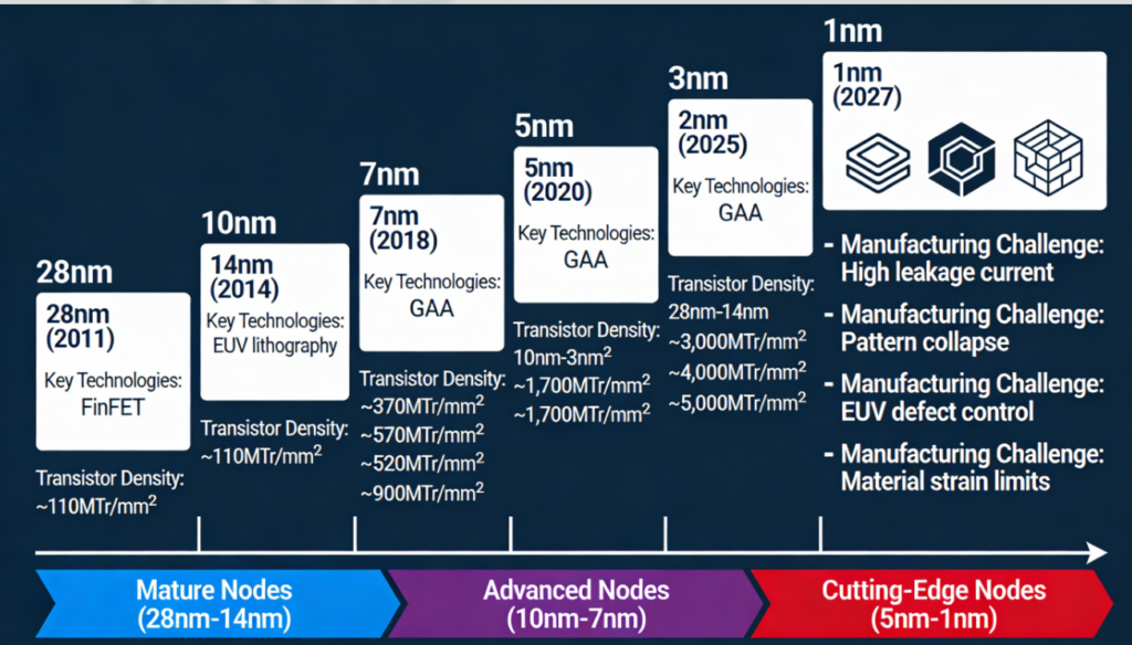
The technological trend in the industry keeps moving towards smaller transistors:
- 3mm manufacturing: In progress (TSMC, Samsung)
- 2nm development: Expected 2025-2026
- 1nm research: Targeting 2027-2029
- Sub-1nm: Theory, observed as an ultimate limit of fundamental physics.
Since features should be in the order of atomic scales (3nm [?] 12 silicon atoms), quantum effects become problematical. Electrons begin to tunnel through the barriers at which they are not supposed. The solution consists of new architectures:
Gate-All-Around (GAA) transistors: Substitute the fin-based design of FinFET with nanosheets, which enhances better electrostatic control.
Backside power delivery Backside power delivery Backside power setup Unoccupied metal Routes supply the power to the back, clearing up metal layers and lowering resistance.
These inventions merely purchase time but pure planar scaling is hampered by hard limits at about 0.5nm. In addition to that, the industry moves to 3D integration and new materials such as graphene.
In-Memory Computing and Memristor.
Resistors that have memory could change computing because they allow calculating in memory structures. The existing computers divide processing and storage and consumed colossal amounts of energy to relocate the data back and forth.
Memristor benefits:
- The increased density with crossed arrays of crossbar.
- non volatile operation (data is stored even without power)
- Capability of analog computing.
- High-level energy efficiency in work-loads.
Issues still exist: resistance variability, switching variability, endurance. It is not yet fit to be mass-produced, but research is still being developed.
All Round Resource Guide to Deeper Learning.
After getting acquainted with this area, here are the resources I found to be really helpful in that order:
To start (No talking presuppositions)
Purdue Semiconductor Fabrication 101: This is a 35-hour self-paced course at Purdue, UT Austin, and Intel on the basics of manufacturing. The vFabLab virtual reality cleanroom simulation is actually cool. Free with certificate.
MIT OpenCourseWare 2,000+ online courses with course lists such as digital systems basics, VLSI design, etc. Provided lecture notes, problem sets and examinations. Enterprise level learning.
Intermediate (Some Technical Background)
Introduction to Chip design with open-source EDA Tools: Hands-on chip design with KiCAD, NGSPICE, and OpenROAD. Coursera. audit at will, includes design workflow concept-to-layout. 3-6 weeks to complete.
The Silicon Free VLSI Courses: VLSI design flow, RISC-V architecture and verification methodology. Industry-relevant and self-paced curriculum.
Advanced (Career Development)
Nordic people developer training: Semiconductor and embedded systems training in which there are hands-on exercises and quizzes. Diploma of completion on completion.
SEMI University Webinars: The free on-demand series on advanced manufacturing, yield management, EUV lithography, and quantum-safe cryptography. Industry-focused perspective.
Relating the Dots: In-Premises Steering.
The basics are in this guide, however, semiconductor technology moves into expertise fields. Here’s how the topics connect:
GENERAL CHIPSET ESSentials: The basics discussed here include chipset architecture, its development, and component count, among others, universally.
MOBILE & CONSUMER CHIPSETS: An extension to the mobile chipset above section based on the development of concrete SoC design, benchmarking, and feature comparison.
Deskktop CHIPsets and LAPTOP: This is a supplement to the desktop/laptop debate where platform choices, upgradeability and optimization of performance are addressed.
CHIPSETs cookie: Go deeper into TPUs, neuromorphic computing, and data center accelerators that were announced in the AI part.
Industry chips: A closer look at automotive, aerospace, medical and other industrial opportunities beyond the summary above.
Emerging Technologies & Trends: More in-depth reporting on quantum computing, photonics and memristors were described in the future trends section.
REAL-life instructions and comparisons: Practical information – the selection of chipsets, interpretation of specifications and practical testing provisions.
Last Reflections: Why This Is Important.
Three months ago, I knew of chipsets as black boxes. I now understand the fact that they form the basis of pretty much everything modern, including the phone in my pocket and the autonomous vehicles on the road, up to the AI systems that are changing industries.
The semiconductor industry is on the crossroads. Days of gearing down the curve easily have gone. The future lies in the technical side of architecture 3D stacking, chiplets, special-purpose accelerators, and possibly something entirely new, such as neuromorphic and quantum computing.
The timing of this field is impressive to any individual who thinks of the same. Billions of dollars are being spent by governments of the world on production of chips domestically. The existing learning resources, such as free university classes and open-source design tools, industry certifications, have decentralized knowledge formerly behind corporate and academic fence lines.
You want to know what your code is implemented on, you may be a student and you have some questions about what you really would like to pursue, or maybe you are simply interested in knowing more about the technology that is changing our world, then the semiconductor industry will provide you with that depth that will keep your curiosity satiated.
All the appliances that you have are years of innovation against millimeters of silicon. That is quite amazing on its part.
The motivation behind the way chips work? to get to know chiplets, process nodes and dedicated accelerators requires time, but it is actually fascinating. Welcome to philosophy, by the way, you can begin with the Purdue Semiconductor Fabrication 101, with the listings of free course offerings at MIT. You will not believe the speed at which the pieces begin to put together.
Be Finishing with As mentioned specific chipset type? See our comprehensive markets on mobile chipsets and AI accelerators. and others emerging technology – each expands on its specific use and its practical implementations.
Read:
Top PDF Annotation Tools: I Tested 5 So You Don’t Have To
I’m software engineer and tech writer with a passion for digital marketing. Combining technical expertise with marketing insights, I write engaging content on topics like Technology, AI, and digital strategies. With hands-on experience in coding and marketing.